Have you ever wondered how the incredibly tiny components on a circuit board get placed so precisely? How a device as slim as a modern smartphone can pack so much computing power into such a small space? The answer lies largely in a manufacturing process called SMT assembly. It’s one of the most important technologies in modern electronics — and yet most people have never heard of it.
In this article, we’ll break down what SMT assembly is, how it works, why it matters, and what makes it the preferred choice for electronics manufacturers around the world.
What Is SMT Assembly?
SMT stands for Surface Mount Technology. SMT assembly is the process of mounting electronic components directly onto the surface of a printed circuit board (PCB), rather than threading component leads through holes drilled in the board.
Before SMT became widespread, electronics manufacturers used a method called through-hole technology (THT), where components had long metal leads that were inserted into holes in the PCB and soldered on the other side. This worked well for many years, but it had limitations — components took up more space, boards were heavier, and the process was slower and more labor-intensive.
SMT changed all of that. Surface mount components — often called SMDs (Surface Mount Devices) — are much smaller, have no leads or very short leads, and are soldered directly onto pads on the board’s surface. This allows for faster production, smaller and lighter boards, and more components packed into a given area.
Today, SMT assembly is the dominant method used in the production of virtually all modern electronic devices — from smartphones and laptops to medical equipment, automotive electronics, and industrial control systems.
A Brief History of SMT Assembly
Surface mount technology was first developed in the 1960s by IBM for use in the guidance computers of the Saturn V rocket. However, it didn’t become widely adopted in commercial electronics until the 1980s, when advances in component miniaturization and automated assembly equipment made it practical and cost-effective.
By the 1990s, SMT had largely replaced through-hole technology for most electronic components. Today, it continues to evolve, enabling ever-smaller components and denser circuit designs that power the latest generation of electronic devices.
How Does SMT Assembly Work?
The SMT assembly process is a carefully orchestrated sequence of steps, most of which are highly automated. Here’s how it works from start to finish:
Step 1: Solder Paste Printing The process begins with applying solder paste to the PCB. A thin metal stencil — with openings precisely cut to match the solder pads on the board — is placed over the PCB. Solder paste (a mixture of tiny solder particles and flux) is then spread across the stencil using a squeegee. When the stencil is lifted, solder paste remains only on the designated pads.
This step is critical. Too much or too little solder paste, or paste applied in the wrong location, can cause defects that are difficult to fix later.
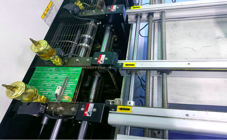
Step 2: Component Placement Next, automated pick-and-place machines take over. These high-speed robotic systems pick up individual SMD components from reels, trays, or tubes and place them onto the solder paste with extraordinary precision — often placing thousands of components per hour.
Modern pick-and-place machines use vision systems to verify the position and orientation of each component before placement. This ensures accuracy even for the smallest components, such as 0201 resistors (which are roughly 0.6mm x 0.3mm — smaller than a grain of sand).
Step 3: Reflow Soldering Once all components are placed, the board moves through a reflow oven. The oven heats the board according to a carefully controlled temperature profile, passing through several zones:
- Preheat zone: Gradually raises the board temperature to avoid thermal shock
- Soak zone: Stabilizes the temperature and activates the flux in the solder paste
- Reflow zone: Reaches peak temperature, melting the solder particles and forming permanent solder joints
- Cooling zone: Slowly cools the board to solidify the solder joints
The result is a board with all components firmly and electrically connected to their respective pads.
Step 4: Inspection After reflow soldering, the boards undergo thorough inspection to identify any defects. Common inspection methods include:
- Automated Optical Inspection (AOI): Cameras scan the board and compare it against a reference image to detect missing components, misalignment, or solder defects
- X-ray Inspection: Used for components where solder joints are hidden beneath the package, such as Ball Grid Arrays (BGAs)
- Manual Visual Inspection: For complex or critical assemblies, trained technicians may visually inspect boards as an additional check
Step 5: Testing Beyond visual inspection, functional testing verifies that the assembled board actually works as intended. In-circuit testing (ICT) checks individual components and connections, while functional testing simulates real-world operating conditions to confirm overall board performance.
Step 6: Rework (if needed) Any boards that fail inspection or testing are sent for rework — a process where defective solder joints are repaired or incorrectly placed components are removed and replaced. Skilled technicians use specialized tools such as hot air rework stations and soldering irons to carry out repairs without damaging the surrounding components.
Key Advantages of SMT Assembly
SMT assembly has become the industry standard for good reason. Here are its most important benefits:
Miniaturization: SMD components are significantly smaller than their through-hole counterparts. This allows manufacturers to create smaller, thinner, and lighter products without sacrificing functionality.
Higher Component Density: Because components are mounted on both sides of the board and packed more closely together, SMT allows far more components per unit area compared to through-hole technology.
Faster Production: Automated pick-and-place machines can place thousands of components per hour, making SMT assembly much faster and more scalable than manual assembly methods.
Lower Cost at Scale: While the initial investment in SMT equipment is significant, the high speed and automation of the process translate into lower per-unit costs at volume, making it highly cost-effective for mass production.
Better Electrical Performance: Shorter component leads mean lower inductance and resistance, which improves high-frequency electrical performance — an important factor in modern high-speed electronics.
Reliability: When done correctly, SMT solder joints are highly reliable. The process is well-understood and tightly controlled, leading to consistent quality across large production runs.
SMT Assembly vs. Through-Hole Technology
While SMT has become dominant, through-hole technology hasn’t disappeared entirely. Some components — particularly large connectors, transformers, and electrolytic capacitors — are still available only in through-hole form. And in applications where mechanical strength is critical (such as connectors that will be frequently plugged and unplugged), through-hole mounting provides a stronger physical bond.
As a result, many modern PCBs use a combination of both SMT and through-hole assembly, getting the best of both worlds. The SMT components provide density and performance, while through-hole components provide mechanical strength where needed.
SMT Assembly in Today’s World
The demand for SMT assembly is growing rapidly, driven by trends across several industries:
Consumer Electronics: Smartphones, tablets, smartwatches, and wireless earbuds all rely heavily on SMT to pack maximum functionality into minimum space.
Automotive Electronics: Modern vehicles contain dozens of electronic control units (ECUs) managing everything from engine performance to safety systems. SMT is essential for producing these boards reliably and at scale.
Medical Devices: Wearable health monitors, diagnostic equipment, and implantable devices require the miniaturization and precision that only SMT can deliver.
IoT and Smart Devices: The explosion of Internet of Things devices — smart home products, industrial sensors, connected appliances — is generating enormous demand for compact, low-cost PCBs produced via SMT assembly.
5G Infrastructure: The rollout of 5G networks requires vast quantities of high-performance PCBs for base stations, antennas, and network equipment — all assembled using advanced SMT processes.
Conclusion
SMT assembly is the invisible engine behind the modern electronics revolution. It’s the reason our devices keep getting smaller, smarter, and more powerful, while also becoming more affordable. From the circuit board in your smartphone to the control systems in electric vehicles, SMT assembly is at work — quietly connecting our world one solder joint at a time. For businesses looking to manufacture high-quality electronics at scale, partnering with a trusted China SMT assembly provider offers a compelling combination of advanced manufacturing capabilities, technical expertise, competitive pricing, and the production capacity to meet the demands of today’s fast-moving electronics market.